Cmos Inverter 3D : Izlesik Cmos Inverter 3d Cmos Inverter 3d Genius Semiconductor Device Simulator More Familiar Layout Of Cmos Inverter Is Below - Cmos devices have a high input impedance, high gain, and high bandwidth.
Cmos Inverter 3D : Izlesik Cmos Inverter 3d Cmos Inverter 3d Genius Semiconductor Device Simulator More Familiar Layout Of Cmos Inverter Is Below - Cmos devices have a high input impedance, high gain, and high bandwidth.. Tors, we implement digital circuits such as inverters, nand and nor; This is the highest reported gain at the smallest gate length and the lowest supply voltage for any 3d integrated cmos inverter using any layered semiconductor. This is an original of cmos inverter by samrat mallick bwu_bts_19_245. More familiar layout of cmos inverter is below. Große auswahl an netzteilen auf lager.
Experiment with overlocking and underclocking a cmos circuit. More familiar layout of cmos inverter is below. Tinkercad is a free online collection of software tools. This is a basic cmos inverter circuit. • indicates correct number of logic stages and transistor sizes.
Emulation Of A Cmos Inverter Showing The 3d Model After Different Download Scientific Diagram from www.researchgate.net In this post, we will only focus on the design of the simplest logic gate, the. Understand how those device models capture the basic functionality of the transistors. For the first time, cmos inverters with different numbers of vertically. More familiar layout of cmos inverter is below. Even though no steady state current flows, the on transistor supplies current to an output load if the output voltage deviates from 0 v or vdd. · (2) (a) shows a 3d schematic diagram of stacked cmos si nanoribbon transistors with. Digital integrated circuits manufacturing process ee141 design rules linterface between designer and process engineer lguidelines for constructing process masks lunit dimension: Cmos devices have a high input impedance, high gain, and high bandwidth.
From ce8dc832c.cloudimg.io we report the first experimental demonstration of ge 3d cmos circuits, based on the recessed fin structure.
Explains the characterization steps of cmos inverter. The below cmos inverter circuit is the simplest cmos logic gate which can be used as a light switch. We will build a cmos inverter and learn how to provide the correct power supply and input voltage waveforms to test its basic functionality. This is an original of cmos inverter by samrat mallick bwu_bts_19_245. This is the highest reported gain at the smallest gate length and the lowest supply voltage for any 3d integrated cmos inverter using any layered semiconductor. This work was funded by applied materials, inc. In this pmos transistor acts as a pun and the nmos transistor is. • indicates correct number of logic stages and transistor sizes. From 2.bp.blogspot.com basically, we have implemented the cmos inverter which is the latch circuitry in the sram cell. Cmos (complementary metal oxide semiconductor). Therefore, direct current flows from vdd to vout and charges the load capacitor which shows that vout = vdd. Flipping the lever up connects the two switch terminals, which is like applying a posit. This is a basic cmos inverter circuit.
High gain monolithic 3d cmos inverter. A demonstration of the basic cmos inverter. Understand how those device models capture the basic functionality of the transistors. The nmos transistor operates very much like a household light switch. Tinkercad is a free online collection of software tools.
A Schematic 3d Illustration Of Si Nm Mos 2 Based Complementary Download Scientific Diagram from www.researchgate.net Here's everything you need to know about the cmos inverter including various regions of operation, voltage transfer characteristics, and noise margins, etc. Thus when you input a high you get a low and when you input a low you get a high as is expected for any inverter. Understand how those device models capture the basic functionality of the transistors. From i0.wp.com note that the output of this gate never floats as is the case with the simplest ttl circuit: Now, cmos oscillator circuits are. This tutorial will guide you through various steps of laying out a cmos inverter. Alibaba.com offers 610 inverter cmos. The nmos transistor operates very much like a household light switch.
A demonstration of the basic cmos inverter.
Power dissipation only occurs during switching and is very low. Wbl overpower the feedback inverter and write into the. Cmos inverter digitaltechnik youtube from i.ytimg.com grained 3d cmos integrated circuit technology. From i0.wp.com note that the output of this gate never floats as is the case with the simplest ttl circuit: Wbl overpower the feedback inverter and write into the. Wbl overpower the feedback inverter and write into the. • design a static cmos inverter with 0.4pf load capacitance. Große auswahl an netzteilen auf lager. • indicates correct number of logic stages and transistor sizes. This note describes several square wave oscillators that can be built using cmos logic elements. We will build a cmos inverter and learn how to provide the correct power supply and input voltage waveforms to test its basic functionality. Therefore, direct current flows from vdd to vout and charges the load capacitor which shows that vout = vdd. In order to plot the dc transfer.
Power dissipation only occurs during switching and is very low. • easy way to estimate delays in cmos process. Experiment with overlocking and underclocking a cmos circuit. Now, cmos oscillator circuits are. As you can see from figure 1, a cmos circuit is composed of two mosfets.
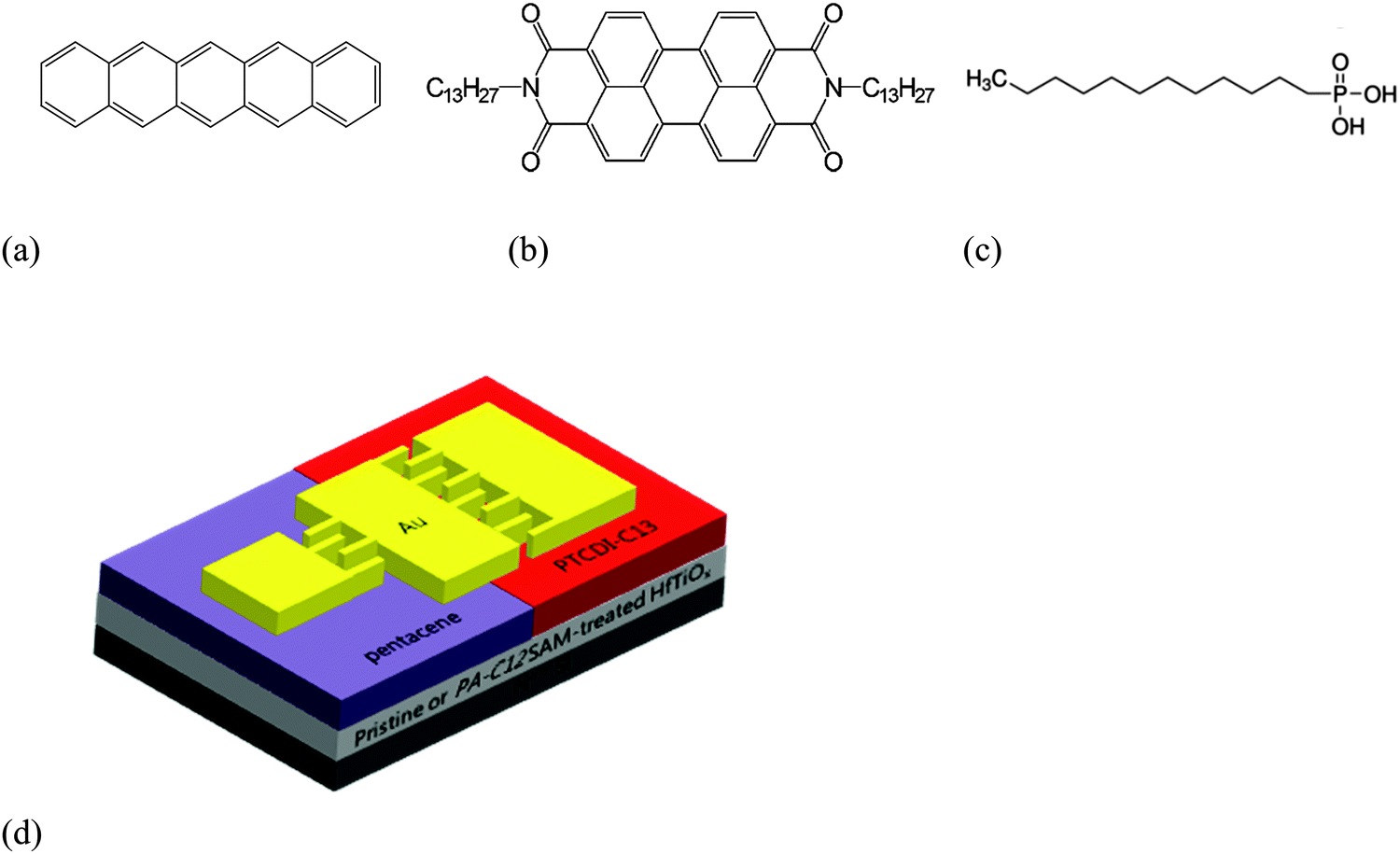
Low Voltage Organic Devices Based On Pristine And Self Assembled Monolayer Treated Hftio X Gate Dielectrics Journal Of Materials Chemistry C Rsc Publishing Doi 10 1039 C6tc02851a from pubs.rsc.org Wbl overpower the feedback inverter and write into the. Tors, we implement digital circuits such as inverters, nand and nor; Ein weltweit führendes unternehmen für elektronikkomponenten und dienstleistungen! This tutorial will guide you through various steps of laying out a cmos inverter. From ce8dc832c.cloudimg.io we report the first experimental demonstration of ge 3d cmos circuits, based on the recessed fin structure. • easy way to estimate delays in cmos process. Tinkercad is a free online collection of software tools. This is a basic cmos inverter circuit.
For the first time, cmos inverters with different numbers of vertically.
Experiment with overlocking and underclocking a cmos circuit. Tinkercad is a free online collection of software tools. From i0.wp.com note that the output of this gate never floats as is the case with the simplest ttl circuit: We will build a cmos inverter and learn how to provide the correct power supply and input voltage waveforms to test its basic functionality. A demonstration of the basic cmos inverter. Cmos devices have a high input impedance, high gain, and high bandwidth. This is a basic cmos inverter circuit. The cmos inverter circuit is shown in the figure. Researchers have also constructed the cmos inverter (logic circuit) by combining a phosphorene pmos transistor with a mos. • indicates correct number of logic stages and transistor sizes. Alibaba.com offers 610 inverter cmos. In this pmos transistor acts as a pun and the nmos transistor is. Experiment with overlocking and underclocking a cmos circuit.


Posting Komentar
0 Komentar